- 您现在的位置:买卖IC网 > Sheet目录344 > MSC8126ADSE (Freescale Semiconductor)KIT ADVANCED DEV SYSTEM 8126
Electrical Characteristics
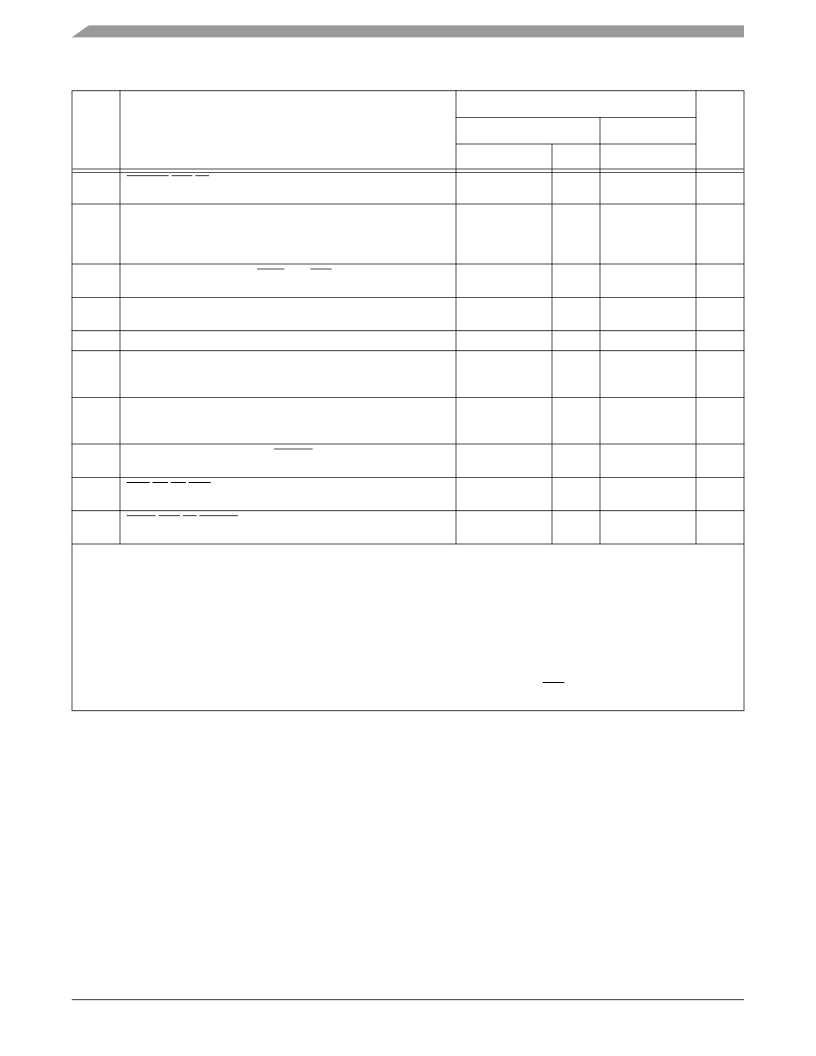
Table 15. AC Timing for SIU Outputs (continued)
Value for Bus Speed in MHz
No.
Characteristic
Ref = CLKIN
133
166
Ref = CLKOUT
133
Units
31
PSDVAL/TEA/TA max delay from the 50% level of the REFCLK
4.9
4.9
5.8
ns
rising edge
32a
Address bus max delay from the 50% level of the REFCLK rising
edge
? Multi-master mode (SIUBCR[EBM] = 1)
? Single-master mode (SIUBCR[EBM] = 0)
5.5
4.2
5.5
3.9
6.4
5.1
ns
ns
32b
Address attributes: TT[0–1]/TBST/TSZ/GBL max delay from the 50%
5.1
5.1
6.0
ns
level of the REFCLK rising edge
32c
Address attributes: TT[2–4]/TC max delay from the 50% level of the
5.7
5.7
6.6
ns
REFCLK rising edge
32d
BADDR max delay from the 50% level of the REFCLK rising edge
4.2
4.2
5.1
ns
33a
Data bus max delay from the 50% level of the REFCLK rising edge
? Data-pipeline mode
? Non-pipeline mode
3.9
6.1
3.7
6.1
4.8
7.0
ns
ns
33b
DP max delay from the 50% level of the REFCLK rising edge
? Data-pipeline mode
? Non-pipeline mode
5.3
6.5
5.3
6.5
6.2
7.4
ns
ns
34
Memory controller signals/ALE/CS[0–4] max delay from the 50%
4.2
3.9
5.1
ns
level of the REFCLK rising edge
35a
DBG/BG/BR/DBB max delay from the 50% level of the REFCLK
4.7
4.7
5.6
ns
rising edge
35b
AACK/ABB/TS/CS[5–7] max delay from the 50% level of the
4.5
4.5
5.4
ns
REFCLK rising edge
Notes:
24
1.
2.
3.
4.
Values are measured from the 50% level of the REFCLK rising edge to the 50% signal level and assume a 20 pF load except
where otherwise specified.
Except for specification 30, which is specified for a 10 pF load, all timings in this table are specified for a 20 pF load.
Decreasing the load results in a timing decrease at the rate of 0.3 ns per 5 pF decrease in load. Increasing the load results in
a timing increase at the rate of 0.15 ns per 5 pF increase in load.
The maximum bus frequency depends on the mode:
In 60x-compatible mode connected to another MSC8126 device, the frequency is determined by adding the input and output
longest timing values, which results in the total delay for 20 pF output capacitance. You must also account for other
influences that can affect timing, such as on-board clock skews, on-board noise delays, and so on.
? In single-master mode, the frequency depends on the timing of the devices connected to the MSC8126.
? To achieve maximum performance on the bus in single-master mode, disable the DBB signal by writing a 1 to the
SIUMCR[BDD] bit. See the SIU chapter in the MSC8122 Reference Manual for details.
MSC8126 Quad Digital Signal Processor Data Sheet, Rev. 15
Freescale Semiconductor
发布紧急采购,3分钟左右您将得到回复。
相关PDF资料
MSC8144ADS
ADS FOR MSC8144 DEVICE
MSC8156EVM
EVAL MODULE FOR MSC8156 LC
MSL1060AW
IC LED DRIVER 6 STRING
MSL1061AV
IC LED DRIVER 6 STRING
MSL2041GU
IC LED DRIVER 4 STRING
MSL2100BR
IC LED DRIVER 8 STRING
MSL2160DQ
IC LED DRIVER 16 STRING
MSL2162DQ
IC LED DRIVER 16 STRING
相关代理商/技术参数
MSC8126MP8000
功能描述:DSP 16BIT 500MHZ MULTI 431FCPBGA RoHS:否 类别:集成电路 (IC) >> 嵌入式 - DSP(数字式信号处理器) 系列:StarCore 标准包装:40 系列:TMS320DM64x, DaVinci™ 类型:定点 接口:I²C,McASP,McBSP 时钟速率:400MHz 非易失内存:外部 芯片上RAM:160kB 电压 - 输入/输出:3.30V 电压 - 核心:1.20V 工作温度:0°C ~ 90°C 安装类型:表面贴装 封装/外壳:548-BBGA,FCBGA 供应商设备封装:548-FCBGA(27x27) 包装:托盘 配用:TMDSDMK642-0E-ND - DEVELPER KIT W/NTSC CAMERA296-23038-ND - DSP STARTER KIT FOR TMS320C6416296-23059-ND - FLASHBURN PORTING KIT296-23058-ND - EVAL MODULE FOR DM642TMDSDMK642-ND - DEVELOPER KIT W/NTSC CAMERA
MSC8126TMP6400
功能描述:DSP 16BIT 400MHZ MULTI 431FCPBGA RoHS:否 类别:集成电路 (IC) >> 嵌入式 - DSP(数字式信号处理器) 系列:StarCore 标准包装:2 系列:StarCore 类型:SC140 内核 接口:DSI,以太网,RS-232 时钟速率:400MHz 非易失内存:外部 芯片上RAM:1.436MB 电压 - 输入/输出:3.30V 电压 - 核心:1.20V 工作温度:-40°C ~ 105°C 安装类型:表面贴装 封装/外壳:431-BFBGA,FCBGA 供应商设备封装:431-FCPBGA(20x20) 包装:托盘
MSC8126TVT6400
功能描述:IC DSP QUAD 16B 400MHZ 431FCPBGA RoHS:是 类别:集成电路 (IC) >> 嵌入式 - DSP(数字式信号处理器) 系列:StarCore 标准包装:2 系列:StarCore 类型:SC140 内核 接口:DSI,以太网,RS-232 时钟速率:400MHz 非易失内存:外部 芯片上RAM:1.436MB 电压 - 输入/输出:3.30V 电压 - 核心:1.20V 工作温度:-40°C ~ 105°C 安装类型:表面贴装 封装/外壳:431-BFBGA,FCBGA 供应商设备封装:431-FCPBGA(20x20) 包装:托盘
MSC8126VT8000
功能描述:IC DSP QUAD 16B 500MHZ 431FCPBGA RoHS:是 类别:集成电路 (IC) >> 嵌入式 - DSP(数字式信号处理器) 系列:StarCore 标准包装:2 系列:StarCore 类型:SC140 内核 接口:DSI,以太网,RS-232 时钟速率:400MHz 非易失内存:外部 芯片上RAM:1.436MB 电压 - 输入/输出:3.30V 电压 - 核心:1.20V 工作温度:-40°C ~ 105°C 安装类型:表面贴装 封装/外壳:431-BFBGA,FCBGA 供应商设备封装:431-FCPBGA(20x20) 包装:托盘
MSC81325M
制造商:STMICROELECTRONICS 制造商全称:STMicroelectronics 功能描述:RF & MICROWAVE TRANSISTORS AVIONICS APPLICATIONS
MSC81350M
制造商:STMICROELECTRONICS 制造商全称:STMicroelectronics 功能描述:RF & MICROWAVE TRANSISTORS AVIONICS APPLICATIONS
MSC81400M
制造商:STMICROELECTRONICS 制造商全称:STMicroelectronics 功能描述:RF & MICROWAVE TRANSISTORS AVIONICS APPLICATIONS
MSC81402
制造商:STMICROELECTRONICS 制造商全称:STMicroelectronics 功能描述:RF & MICROWAVE TRANSISTORS GENERAL PURPOSE AMPLIFIERS APPLICATIONS
